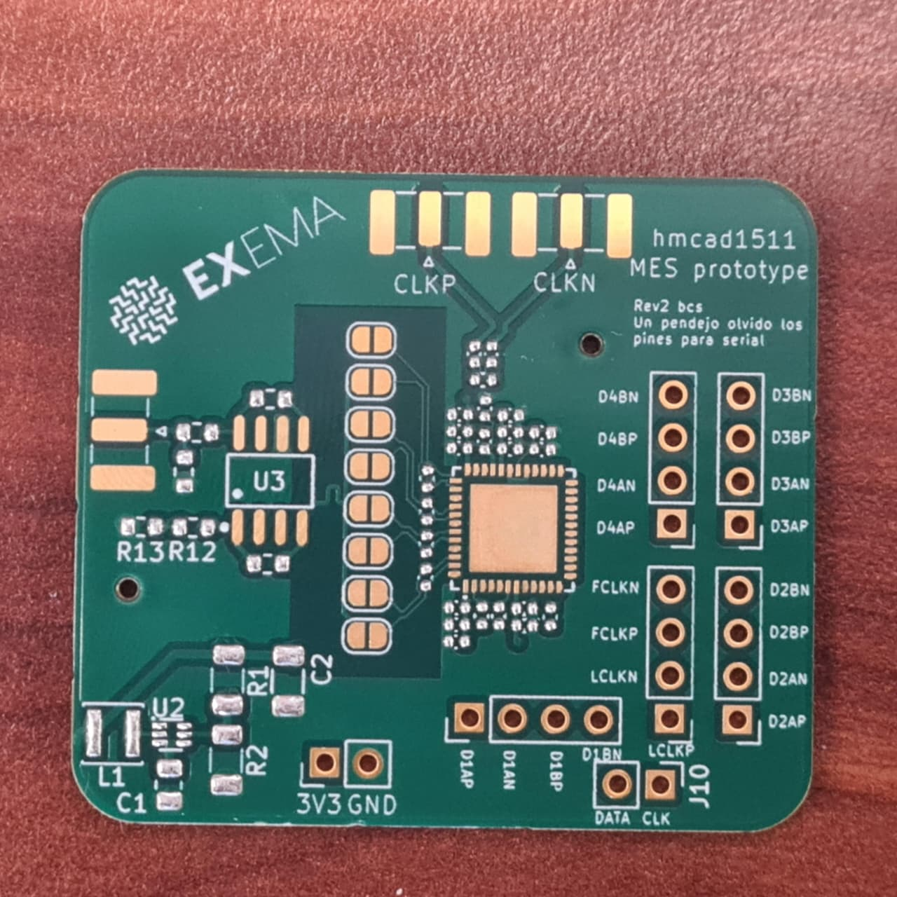
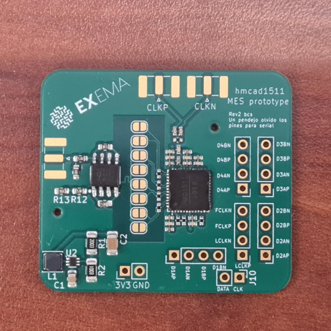
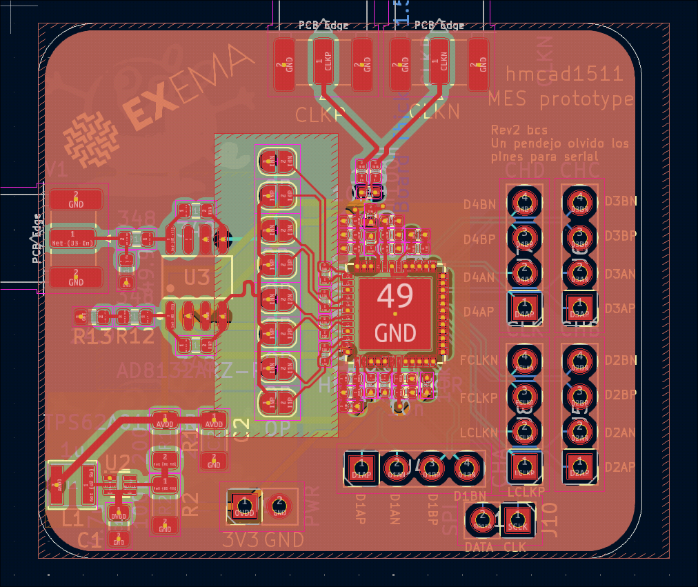
This is an ADC board PCB designed in KiCad. The main goal of this project was to create a high-speed data acquisition system that can be used for measuring fast signals as part of a bigger project involving signal processing. Since I had coupon for six layer PCBs I decided to design this ADC board with a six layer design to ensure proper signal integrity, minimize noise, small form factor and the use of in-pad vias.
Design
The PCB was designed using KiCad using the HMCAD1511TR ADC chip as the main component for data acquisition and the AD8132 differential amplifier for signal conditioning.
Manufacturing
The PCB was manufactured using a professional PCB manufacturing service. The components were soldered using a reflow soldering process to ensure proper connections and reliability also done by the manufacturer since some of the components were pretty much exotic and was a lot cheaper than having to order them separately.